Performance Rating
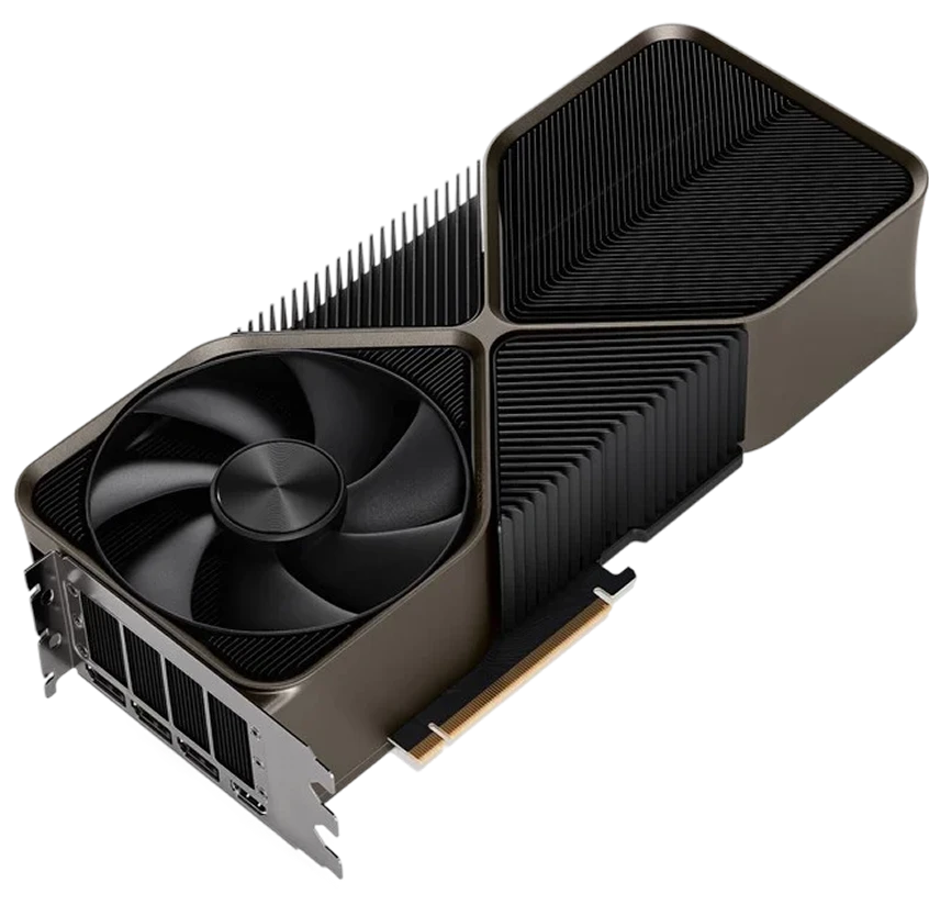
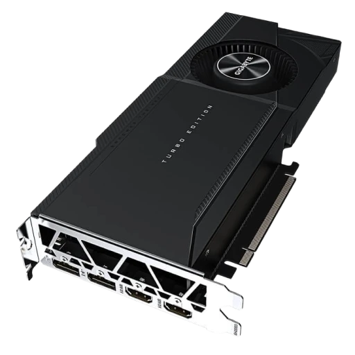
The GeForce RTX 4090 D is an enthusiast-class graphics card by NVIDIA, launched on December 28th, 2023. Built on the 5 nm process, and based on the AD102 graphics processor, in its AD102-250-A1 variant, the card supports DirectX 12 Ultimate. This ensures that all modern games will run on GeForce RTX 4090 D. Additionally, the DirectX 12 Ultimate capability guarantees support for hardware-raytracing, variable-rate shading and more, in upcoming video games. The AD102 graphics processor is a large chip with a die area of 609 mm² and 76,300 million transistors. Unlike the fully unlocked TITAN Ada, which uses the same GPU but has all 18432 shaders enabled, NVIDIA has disabled some shading units on the GeForce RTX 4090 D to reach the product's target shader count. It features 14592 shading units, 456 texture mapping units, and 176 ROPs. Also included are 456 tensor cores which help improve the speed of machine learning applications. The card also has 114 raytracing acceleration cores. NVIDIA has paired 24 GB GDDR6X memory with the GeForce RTX 4090 D, which are connected using a 384-bit memory interface. The GPU is operating at a frequency of 2280 MHz, which can be boosted up to 2520 MHz, memory is running at 1313 MHz (21 Gbps effective).
Contents:
Memory ML Performance Compute Power Architecture & Compatibility ML Software Support Clocks & Performance Power Consumption Rendering Benchmarks AdditionalMemory
Memory Size
Memory Type
Memory Bandwidth
Memory Bus Width
ML Performance
FP16 (Half Precision)
BF16 (Brain Float)
TF32 (TensorFloat)
Compute Power
FP32 (Single Precision)
FP64 (Double Precision)
CUDA Cores
RT Cores
Architecture & Compatibility
GPU Architecture
SM (Streaming Multiprocessor)
PCIe Version
ML Software Support
CUDA Version
Clocks & Performance
Base Clock
Boost Clock
Memory Clock
Power Consumption
TDP/TGP
Recommended PSU
Power Connector
Benchmarks
llama.cpp, llama 7B Q4_0
llama.cpp, llama-2-7b-Q4_0
Geekbench AI, FP16
Geekbench AI, INT8
Geekbench AI, FP32
Additional
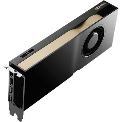
Slots
Release Date
Display Outputs
Renting is cheaper than buying
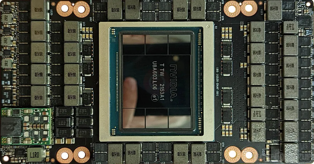
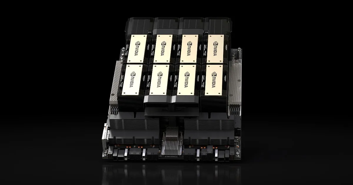
H100 80Gb SXM (80GB)
NVIDIA
Флагманская GPU на архитектуре Hopper с 80 ГБ памяти HBM3 в форм-факторе SXM. Создана для обучения и инференса больших языковых моделей, HPC задач. Поддерживает FP64, FP32, TF32, FP16, BF16, FP8 и INT8 вычисления с Tensor Cores 4-го поколения.
from 299.11 RUB/hour